Indo-Japan Background
NPO Japan-India Business Bureau

Japan-India Semiconductor Committee JISC

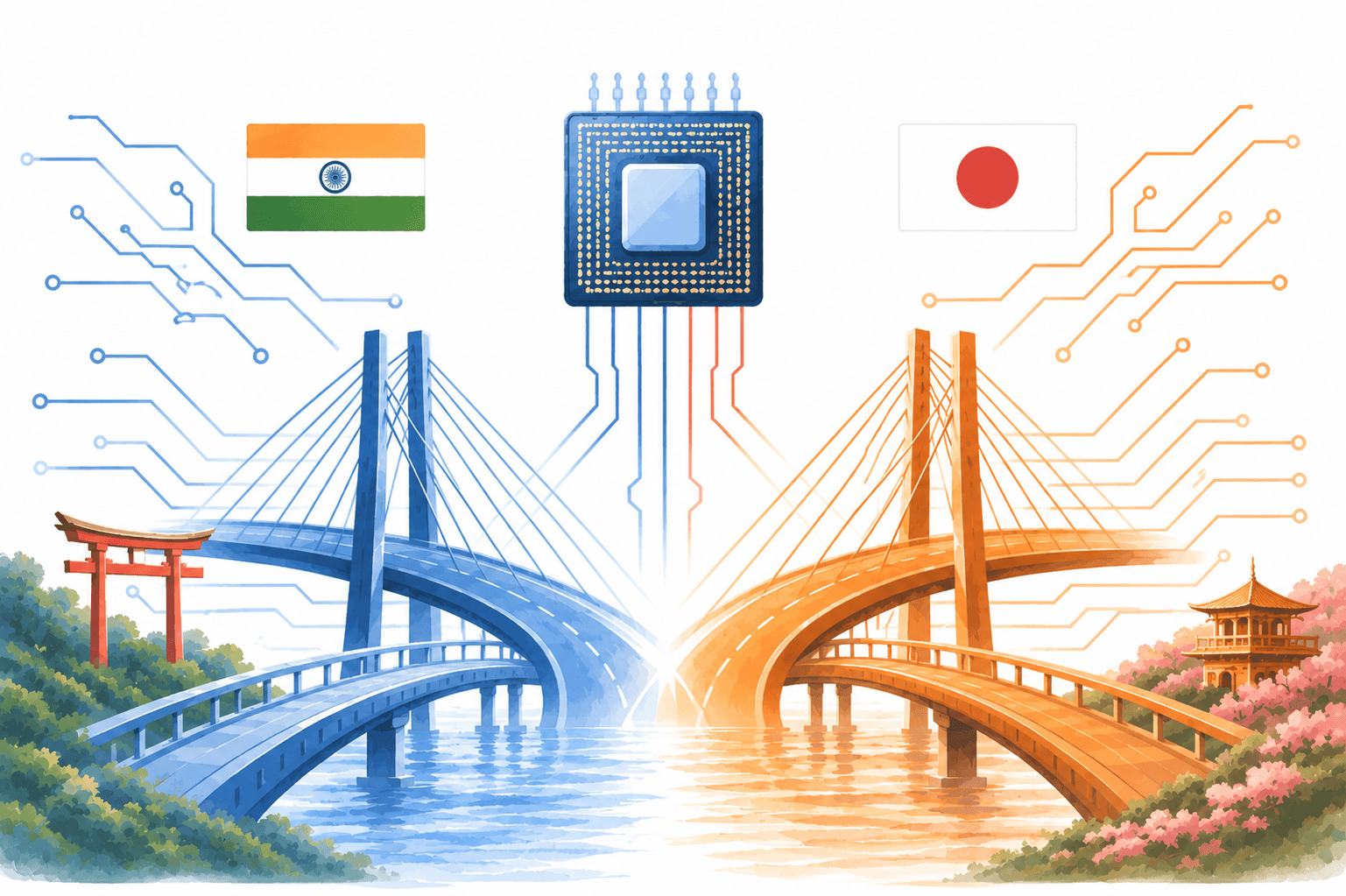
JISC works to strengthen collaboration between industry, government, academia, and technology leaders across the semiconductor ecosystem. Through strategic partnerships, business facilitation, research collaboration, talent development, and market expansion support, JISC aims to accelerate semiconductor growth opportunities between Japan and India.

memory

JISC

Japan-India Semiconductor Committee

location_onIN

JIBB, 6th Floor, 162, Sector 16, Noida, Uttar Pradesh

Strategic Hub Location

location_onJP

Tameike Suzuki Building 3F, 1-2-13 Akasaka, Minato-ku, Tokyo

Strategic Hub Location

Who We Are

The Mission of JISC

The Japan India Semiconductor Committee (JISC), operating under the Japan India Business Bureau (JIBB), aims to strengthen semiconductor collaboration between Japan and India by connecting Japanese technology companies with India’s growing semiconductor ecosystem.

check_circleTechnology partnerships
check_circleManufacturing collaboration
check_circleSemiconductor supply chain development
check_circleInvestment opportunities
check_circleInnovation exchange between Japan and India
Member Companies

Japanese Companies Interested in Indian Semiconductor Ecosystem

Toho Koki Seisakusho Logo

Toho Koki Seisakusho

Japanese precision engineering company specializing in semiconductor-related machining and polishing technologies.

CMP Pad ProcessingSemiconductor Substrate PolishingSurface Inspection SystemsSiC and AlN Semiconductor Materials

Additional Information

Developed advanced semiconductor manufacturing technologies through collaboration with universities and research institutes. Provides CMP pad groove adjustment systems, direct polishing technologies for semiconductor substrates, and solutions for SiC and AlN materials.

languageOfficial Website
Kuraray Logo

Kuraray

Japanese specialty chemicals and advanced materials company with strong semiconductor manufacturing applications.

Semiconductor CMP PadsSemiconductor Fab Water RecyclingFunctional Polymer Materials

Additional Information

Develops next-generation poreless CMP pads for advanced fabrication. Supplies hollow fiber membrane systems for wastewater recycling inside semiconductor fabrication plants.
languageOfficial Website
SUMCO Corporation Logo

SUMCO Corporation
One of the world’s leading manufacturers of silicon wafers used in semiconductor devices.

Silicon WafersSemiconductor Substrate MaterialsAdvanced Wafer Manufacturing

Additional Information

Produces high-purity silicon wafers for logic chips, memory devices, and advanced electronics. Focuses on high quality standards and stable supply chains.

languageOfficial Website
Edwards Japan Limited Logo

Edwards Japan Limited

Provides vacuum and abatement solutions critical for semiconductor manufacturing facilities.

Vacuum PumpsFab Abatement SystemsManufacturing Infrastructure

Additional Information

Supports semiconductor fabs with advanced vacuum systems and exhaust gas treatment technologies. Improves production efficiency, safety, and sustainability.

languageOfficial Website
Okuma Corporation Logo

Okuma Corporation

Precision manufacturing and CNC machine tool company supporting semiconductor and industrial manufacturing.

Ultra-Precision CNC MachiningEquipment ManufacturingSmart Factory Automation

Additional Information

Provides highly accurate CNC machining systems and smart manufacturing solutions. Supports high-precision industrial manufacturing through automation and digital technologies.

languageOfficial Website
TAZMO Co. Ltd. Logo

TAZMO Co. Ltd.

Manufactures semiconductor production equipment and automation systems.

Coater/Developer SystemsCleaning SystemsWafer Transfer EquipmentChemical Supply & Recycling

Additional Information

Develops coater/developer platforms, cleaning equipment, and wafer handling robots. Technologies help improve production efficiency and process stability.

languageOfficial Website
Denka Co. Ltd. Logo

Denka Co. Ltd.

Japanese materials and electronics company offering advanced semiconductor packaging and thermal management materials.

Packaging MaterialsSpherical SilicaThermal Conductive MaterialsSilicon Nitride Products

Additional Information

Supplies materials used in packaging, thermal control, and component manufacturing. Product portfolio includes spherical silica and alumina for improved reliability.

languageOfficial Website
Kyocera Corporation Logo

Kyocera Corporation

Provides ceramic and electronic solutions for semiconductor manufacturing and packaging.

Ceramic PackagesFine Ceramic ComponentsProcessing Equipment ComponentsElectronic Packaging

Additional Information

Manufactures ceramic substrates and packages used in wafer processing. Supports miniaturization, high durability, and reliable electronic packaging.

languageOfficial Website

Global Deep-Tech Corridor

Indo-Japan Semiconductor
Research & Innovation Hub

Noida, Uttar Pradesh

security

Decentralizing the Global Supply Chain

A resilient innovation pipeline to counter geopolitical shifts and foster native "Made in India" deep-tech IP.

location_on

Strategic Hub — Noida, UP

Situated within a premier electronics cluster providing startups with immediate proximity to consumer electronics assembly plants.

school

Synergy of Indian & Japanese Academia

Academic institutions from both nations act as "senders" for high-risk experimentation and early-stage technical know-how.

corporate_fare

Synergy of Indian & Japanese Corporations

Corporate partners provide market scale, rapid pathway integration, and the global pathways required for commercial success.

Semiconductor Applications
rocket_launch

TRL Lifecycle Pipeline

TRL 1–3

Nascent Stage: Research & De-risking

Analytical proof-of-concept and prototyping to lower the barrier to entry for deep tech.

Key Contributors: Academia
TRL 4–6

Validation Stage: Prototype Testing

Moving designs out of controlled labs into simulated environments to ensure functional viability.

Key Contributors: Academia, Corporations
TRL 7–9

Maturity & Commercial Stage: Scaling

Series A/B funding, fabrication access, and integration into automotive and industrial supply chains.

Key Contributors: Corporations
precision_manufacturing

Specialized Physical Environment

The facility provides specialized wet labs and high-end semiconductor fabrication tools beyond basic office space.

biotech

Advanced Testing & Verification Labs

Access to specialized facilities and equipment necessary to verify complex chip designs and prototypes.

menu_book

Specialized Technical Libraries

Curated access to technical documentation, research papers, and essential semiconductor design datasets.

hub

Quad-Pillar Collaborative Model

A synergistic model connecting Indian & Japanese academia and corporations to drive deep-tech innovation at scale.

Government & Industry Partners

JISC is Supported By

India Semiconductor Mission
Invest India
Invest UP
Guidance Tamil Nadu
CII
IESA
ELCINA
India Semiconductor Mission
Invest India
Invest UP
Guidance Tamil Nadu
CII
IESA
ELCINA
Our Strategic Mission

The PURPOSE of JISC

handshake

Japanese Corporate Collaboration

Accelerating collaboration in both domestic and global markets through partnerships with international organizations, supported by exhibitions, industry conferences, and government-led initiatives.

01
public

India-International Cooperation

Promoting technology collaboration and company matching between Indian and international companies and academic institutions, along with industry-academia-government collaboration.

02
trending_up

Market Trend Research

Research on market and technology trends in the Indian semiconductor and electronic components industry, providing information difficult to obtain through media sources.

03
biotech

Technology Development

Promotion of technology transfer, licensing, and collaboration opportunities for joint ventures, enhancing inter-country development through regular technical presentations.

04
storefront

Marketing & Promotion

Inter-company collaboration in marketing and promotion in the Indian market overcomes the limitations of entering the market alone. Working as a unified effort.

05
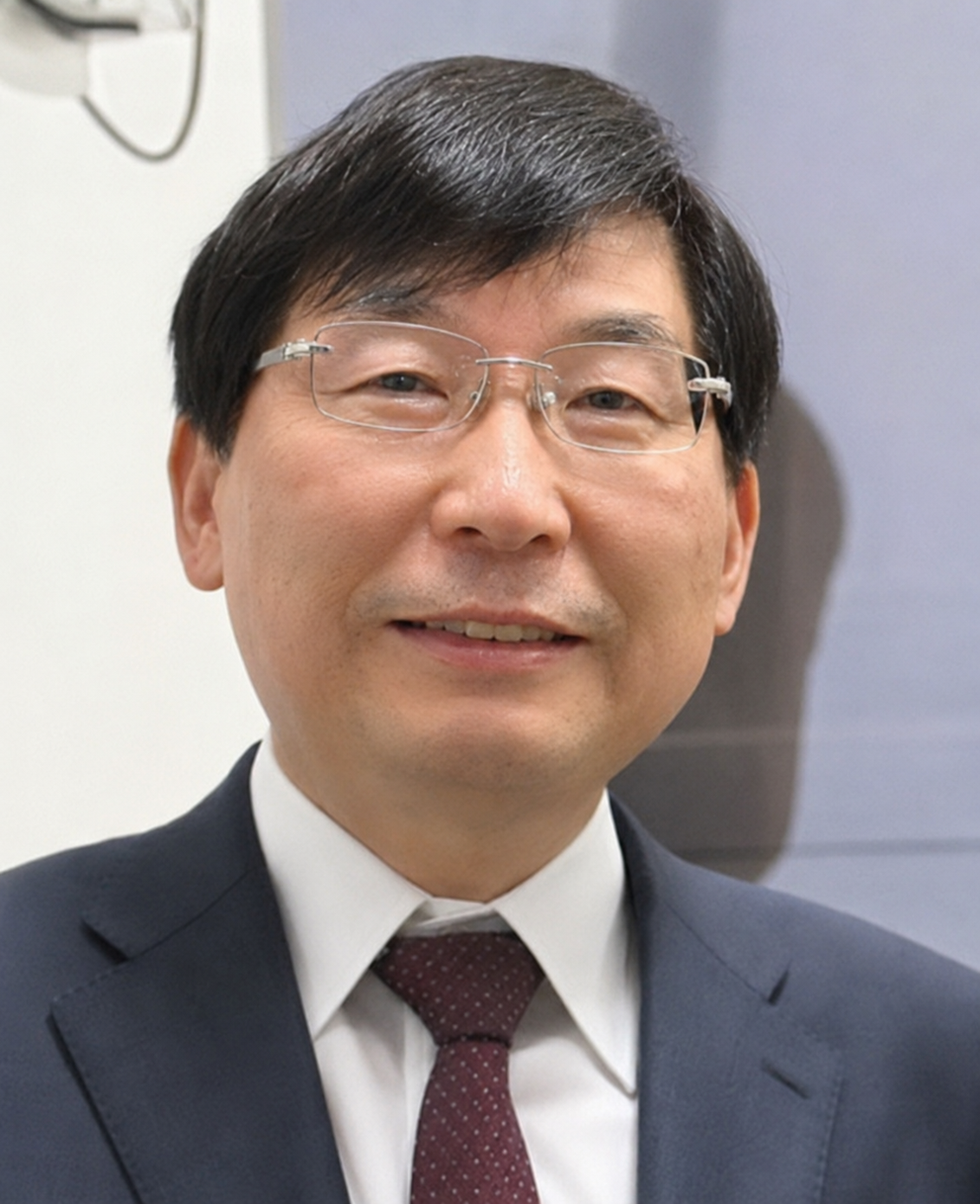
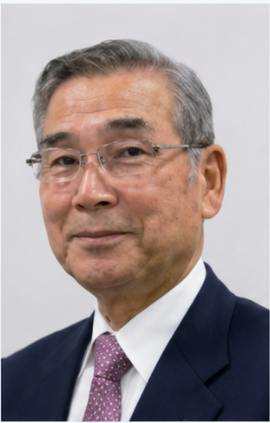
Tatsutoshi Suzuki

Greetings

Tatsutoshi Suzuki

JISC Chairman·Planarization CMP Technology Study Group Chairman·Toho Steel Works Chairman

Although Japan's semiconductor industry has fallen from its former top share, it still boasts world-class strengths in manufacturing equipment and materials, with a strong presence in power semiconductors and image sensors. It is in a transitional period aiming for renewed growth through investment in cutting-edge fields and international collaboration.

As the semiconductor industry expands globally, India is attracting attention as the "factory of the world" in conjunction with the movement to decouple from China. Under the "Make in India" policy, the country is promoting rapid technological development with the aim of domestic semiconductor production.

Advisory & Committee Members

Leading Industry Experts

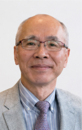
Toshiro Doi

Toshiro Doi

Honorary Director

  • Professor Emeritus, Kyushu University
  • Professor Emeritus, Saitama University
  • Member, Engineering Academy of Japan (EAJ)
  • Visiting Researcher, RIKEN
  • Fellow and Honorary Member, Japan Society for Precision Engineering (JSPE)
  • Founder and Honorary Chairman, Planarization CMP Special Committee, JSPE
  • Chairman and Advisor, Optical Components Production Technology Division, JOEM

Toshiro Doi

add
Masaharu Kinoshita (Seiji Kinoshita)

Masaharu Kinoshita (Seiji Kinoshita)

President & CEO, Kinoshita Consulting

  • Former Chief Executive Officer, Nitta Haas Incorporated
  • Former Chief Executive Officer, Toshiba Corporation
  • President & Chief Executive Officer, Kinoshita Consulting
  • Doctor of Engineering, The University of Tokyo

Masaharu Kinoshita (Seiji Kinoshita)

add
Hirokuni Hiyama

Hirokuni Hiyama

Technical Advisor, Ebara Corporation

  • Fellow and Technical Advisor, Ebara Corporation
  • Member, Semiconductor Equipment Association of Japan (SEAJ)
  • Recipient of the ICPT Society Award (2025)

Hirokuni Hiyama

add
Shuhei Kurokawa

Shuhei Kurokawa

Professor, Kyushu University

  • Professor, Department of Mechanical Engineering, Kyushu University
  • Fellow and Representative Member, Japan Society of Mechanical Engineers (JSME)
  • Vice President, Director, and Fellow, Japan Society for Precision Engineering (JSPE)

Shuhei Kurokawa

add
Kazuto Yamauchi

Kazuto Yamauchi

Professor, Osaka University

  • Specially Appointed Full-Time Professor, Osaka University & RIKEN
  • Member, Optical Society of Japan
  • Member, Japanese Society for Synchrotron Radiation Research
  • Member, Japan Society of Applied Physics
  • Former President, Japan Society for Precision Engineering (JSPE)

Kazuto Yamauchi

add
Seiichi Kondo

Seiichi Kondo

Committee Member, SIA

  • Committee Member, Semiconductor Industry Association (SIA)
  • Fellow and Ph.D., Resonac Holdings Corporation
  • Specialist in Planarization CMP Technology Research

Seiichi Kondo

add
Hideto Miyake

Hideto Miyake

Professor, Mie University

  • Professor, Department of Electrical and Electronic Engineering, Mie University
  • Director and Chairman, Wide-Gap Semiconductor Society
  • Member, Japanese Association for Crystal Growth

Hideto Miyake

add
Yasuhiko Takeno

Yasuhiko Takeno

Committee Member, SIA

  • Committee Member, Semiconductor Industry Association (SIA)
  • Fellow and Ph.D., Resonac Holdings Corporation
  • Committee Member, Planarization CMP Technical Research Group

Yasuhiko Takeno

add

Partner Organizations

Powered by JIBB

Office Space

Japan India Business Bureau (NPO)

Get Involved

Building the Semiconductor Future Together